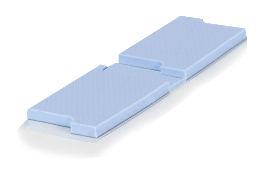
Gap-Filler Pads in The Third Dimension
It is actually the rule that electronic applications consist of a large number of different components. However, these almost always have different heights. Gaps and tolerances are therefore unavoidable. To compensate for these, gap fillers are often used. They minimize the thermal resistance between electronic components and cooling housings or heat sinks. They are available in the form of fluids or as pads. The former have the advantage that virtually no pressure is exerted on components during processing or operation. This is particularly important for mechanically sensitive components. However, these paste-like gap fillers must first polymerize after assembly, i.e. cure.
Another disadvantage is that not every company wants to integrate such a dispensing process into its workflows, partly because procuring the necessary equipment involves a not inconsiderable financial outlay.
The usual alternative is gap-filler pads. But the films commonly used up to now can only be applied with a certain amount of mechanical stress. And the thickness of each pad only fills a certain gap. In other words, when a material thickness is applied to several non-planar electronic components with different heights, there is then a risk of damage, especially to sensitive and delicate components.
Thanks to a new process, we can now adapt some of our gap-filler pads precisely to thickness requirements in three dimensions. In this process, the customer receives a singular composite gap filler pad from us and can thus bypass all dispensing and curing processes. The shape of the pad is tailored to the individual tolerances and heights of the assembly on the board. As a result, all components can be connected in a quasi multiplan manner – regardless of height.
Another advantage of the process is the dielectric safety of the polymerized films, as there is no risk of air bubbles forming after pressing.


